Home
Characterization and production of an electrical device based on graphene
Barnes and Noble
Loading Inventory...
Characterization and production of an electrical device based on graphene in Franklin, TN
Current price: $47.00
Barnes and Noble
Characterization and production of an electrical device based on graphene in Franklin, TN
Current price: $47.00
Loading Inventory...
Size: OS
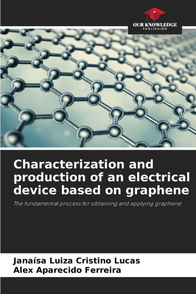
The general objective of the work we are developing consists of the process of fabricating devices in two-dimensional materials, including lithography, metal deposition for electrical contact patterns, morphological characterization and electrical measurements. The sample was produced using a method called Mechanical Cleaving. This method basically consists of manually separating the stacked layers of a graphite crystal repeatedly by sticking and peeling the crystal to a piece of tape. This is then attached to the silicon dioxide substrate and pressed manually so that the flakes adhere to the substrate. The number of layers in the sample was determined by optical microscopy. The sample was also analyzed using Raman spectroscopy. To manufacture the contacts, a LaserWriter LW405 was used for optical lithography, followed by Cr/Au deposition and a lift-off process to finalize the device. Our work aims to understand the basic characteristics of electrical transport, the device fabrication process, electrical measurements and morphological characterization, as well as contributing to the first steps in the process.
The general objective of the work we are developing consists of the process of fabricating devices in two-dimensional materials, including lithography, metal deposition for electrical contact patterns, morphological characterization and electrical measurements. The sample was produced using a method called Mechanical Cleaving. This method basically consists of manually separating the stacked layers of a graphite crystal repeatedly by sticking and peeling the crystal to a piece of tape. This is then attached to the silicon dioxide substrate and pressed manually so that the flakes adhere to the substrate. The number of layers in the sample was determined by optical microscopy. The sample was also analyzed using Raman spectroscopy. To manufacture the contacts, a LaserWriter LW405 was used for optical lithography, followed by Cr/Au deposition and a lift-off process to finalize the device. Our work aims to understand the basic characteristics of electrical transport, the device fabrication process, electrical measurements and morphological characterization, as well as contributing to the first steps in the process.