Home
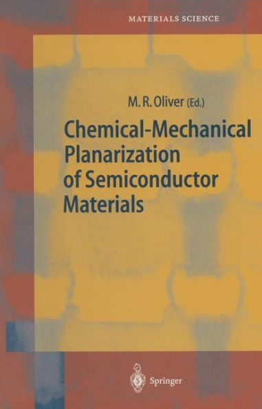
Chemical-Mechanical Planarization of Semiconductor Materials / Edition 1
Barnes and Noble
Loading Inventory...
Chemical-Mechanical Planarization of Semiconductor Materials / Edition 1 in Franklin, TN
Current price: $219.99

Barnes and Noble
Chemical-Mechanical Planarization of Semiconductor Materials / Edition 1 in Franklin, TN
Current price: $219.99
Loading Inventory...
Size: OS
Chemical Mechanical Planarization (CMP) has emerged in the last two decades and grown rapidly as a basic technology widely used in semiconduc tor device fabrication. As a semiconductor processing step, it was developed at IBM in the mid 1980s. From this beginning the technology has been widely adopted throughout the semiconductor industry. As basic CMP technology has been understood and accepted throughout the semiconductor industry, its uses in different parts of the semiconductor process have multiplied. This includes special steps for some special processing flows, such as for DRAM technology. In addition, the availability of CMP technology has enabled the implementation of new technologies, with the best example being copper interconnect technology. Copper could not be practi cally implemented into semiconductor process flows until the advent of CMP. Unfortunately, the rapid acceptance and implementation of CMP technol ogy in wafer fabrication has occurred without a corresponding rate of advance in the underlying science. Progress is being made in understanding the un derlying CMP mechanisms, but, in general, it is slow and uneven. The most noteworthy exception to this trend is the science of metal CMP reactions, where the scientific understanding is actually driving much of the advance of the technology. There has been no corresponding progress in other CMP areas however.
Chemical Mechanical Planarization (CMP) has emerged in the last two decades and grown rapidly as a basic technology widely used in semiconduc tor device fabrication. As a semiconductor processing step, it was developed at IBM in the mid 1980s. From this beginning the technology has been widely adopted throughout the semiconductor industry. As basic CMP technology has been understood and accepted throughout the semiconductor industry, its uses in different parts of the semiconductor process have multiplied. This includes special steps for some special processing flows, such as for DRAM technology. In addition, the availability of CMP technology has enabled the implementation of new technologies, with the best example being copper interconnect technology. Copper could not be practi cally implemented into semiconductor process flows until the advent of CMP. Unfortunately, the rapid acceptance and implementation of CMP technol ogy in wafer fabrication has occurred without a corresponding rate of advance in the underlying science. Progress is being made in understanding the un derlying CMP mechanisms, but, in general, it is slow and uneven. The most noteworthy exception to this trend is the science of metal CMP reactions, where the scientific understanding is actually driving much of the advance of the technology. There has been no corresponding progress in other CMP areas however.


