Home
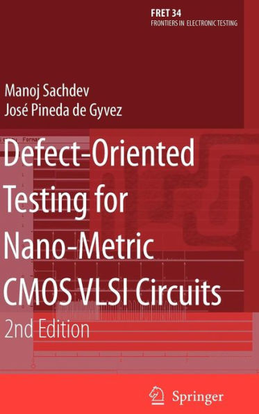
Defect-Oriented Testing for Nano-Metric CMOS VLSI Circuits / Edition 2
Barnes and Noble
Loading Inventory...
Defect-Oriented Testing for Nano-Metric CMOS VLSI Circuits / Edition 2 in Franklin, TN
Current price: $219.99
Barnes and Noble
Defect-Oriented Testing for Nano-Metric CMOS VLSI Circuits / Edition 2 in Franklin, TN
Current price: $219.99
Loading Inventory...
Size: OS
Defect-oriented testing methods have come a long way from a mere interesting academic exercise to a hard industrial reality. Many factors have contributed to its industrial acceptance. Traditional approaches of testing modern integrated circuits have been found to be inadequate in terms of quality and economics of test. In a globally competitive semiconductor market place, overall product quality and economics have become very important objectives. In addition, electronic systems are becoming increasingly complex and demand components of the highest possible quality. Testing in general and defect-oriented testing in particular help in realizing these objectives. For contemporary System on Chip (SoC) VLSI circuits, testing is an activity associated with every level of integration. However, special emphasis is placed for wafer-level test, and final test. Wafer-level test consists primarily of dc or slow-speed tests with current/voltage checks per pin under most operating conditions and with test limits properly adjusted. Basic digital tests are applied and in some cases low-frequency tests to ensure analog/RF functionality are exercised as well. Final test consists of checking device functionality by exercising RF tests and by applying a comprehensive suite of digital test methods such as I , delay fault testing, DDQ stuck-at testing, low-voltage testing, etc. This partitioning choice is actually application dependent.
Defect-oriented testing methods have come a long way from a mere interesting academic exercise to a hard industrial reality. Many factors have contributed to its industrial acceptance. Traditional approaches of testing modern integrated circuits have been found to be inadequate in terms of quality and economics of test. In a globally competitive semiconductor market place, overall product quality and economics have become very important objectives. In addition, electronic systems are becoming increasingly complex and demand components of the highest possible quality. Testing in general and defect-oriented testing in particular help in realizing these objectives. For contemporary System on Chip (SoC) VLSI circuits, testing is an activity associated with every level of integration. However, special emphasis is placed for wafer-level test, and final test. Wafer-level test consists primarily of dc or slow-speed tests with current/voltage checks per pin under most operating conditions and with test limits properly adjusted. Basic digital tests are applied and in some cases low-frequency tests to ensure analog/RF functionality are exercised as well. Final test consists of checking device functionality by exercising RF tests and by applying a comprehensive suite of digital test methods such as I , delay fault testing, DDQ stuck-at testing, low-voltage testing, etc. This partitioning choice is actually application dependent.
