Home
Fundamentals of Device and Systems Packaging: Technologies and Applications, Second Edition / Edition 2
Barnes and Noble
Loading Inventory...
Fundamentals of Device and Systems Packaging: Technologies and Applications, Second Edition / Edition 2 in Franklin, TN
Current price: $225.00

Barnes and Noble
Fundamentals of Device and Systems Packaging: Technologies and Applications, Second Edition / Edition 2 in Franklin, TN
Current price: $225.00
Loading Inventory...
Size: OS
Publisher's Note: Products purchased from Third Party sellers are not guaranteed by the publisher for quality, authenticity, or access to any online entitlements included with the product.
A fully updated, comprehensive guide to microelectronic device and systems packaging principles and practices
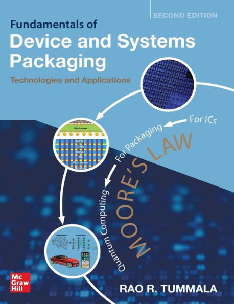
This thoroughly revised book offers the latest, comprehensive fundamentals in device and systems packaging technologies and applications. You will get in-depth explanations of the 15 core packaging technologies that make up any electronic system, including electrical design for power, signal, and EMI; thermal design by conduction, convection,and radiation heat transfer; thermo-mechanical failures and reliability;advanced packaging materials at micro and nanoscales; ceramic, organic, glass,and silicon substrates. This resource also discusses passive components such as capacitors, inductors, and resistors and their proximity integration with actives; chip-to-package interconnections and assembly; wafer and panel embedding technologies; 3D packaging with and without TS; RF and millimeter-wave packaging; role of optoelectronics; mems and sensor packaging;encapsulation, molding and sealing; and printed wiring board and its assembly to form end-product systems.
Fundamentals of Device and Systems Packaging: Technologies and Applications
, Second Edition
introduces the concept of Moore’s Law for packaging, as Moore’s Law for ICs is coming to an end due to physical, material, electrical, and financial limitations. Moore’s Law for Packaging (MLP) can be viewed as interconnecting and integrating many smaller chips with high aggregate transistor density, at higher performance and lower cost than Moore’s Law for ICs. This book lays the groundwork for Moore’s Law for Packaging by showing how I/Os have evolved from one package family node to the next, starting with <16 I/Os in the 1960s with leadframe-plastic packages to the current silicon interposers with about 200,000 I/Os. It proposes a variety of ways to extend Moore’s Law, such as extending Si interposers and beyond using glass panel embedding. As Moore’s Law for Electronic Packaging comes to its end, this book proposes 3D opto-electronics in the short term and, ultimately, Quantum Computing as the next Moore’s Law.


