Open Today
10:00AM - 8:00PM
See Special Hours
Wed-Sat
10:00AM
-
8:00PM
Sun
12:00PM
-
6:00PM
Mon-Tue
10:00AM
-
8:00PM
On Sale
Women
Men
Baby & Kids
Beauty
Home
Easter
Spring Essentials
Graduation
Sustainability
Spring Break
Prom Essentials
Stores
Brands
Wishlist
Wishlist
Items on Sale
Clothing
Tops
Bottoms
Outerwear
Swimwear
Sleepwear
Underwear
Dresses & Jumpsuits
Accessories
Socks
Hosiery
Hats
Headbands
Scarves
Gloves & Mittens
Sunglasses
Eyeglasses
Belts
Wallets
Watches
Jewelry
Shoes
Sneakers
Boots
Sandals
Flip Flops
Pumps
Flats
Shoe Care
Bags & Backpacks
Satchel
Messenger
Saddle
Tote
Duffel
Hobo
Clutch
Sports & Fitness
Yoga
Gym
Outdoor
Sportswear
Items on Sale
Clothing
Tops
Bottoms
Outerwear
Swimwear
Sleepwear
Underwear
Accessories
Socks
Hats
Headbands
Scarves
Gloves & Mittens
Sunglasses
Eyeglasses
Belts
Ties
Wallets
Watches
Jewelry
Shoes
Sneakers
Boots
Sandals
Flip Flops
Dress Shoes
Shoe Care
Bags & Backpacks
Messenger
Duffel
Briefcase
Luggage
Sports & Fitness
Gym
Outdoor
Sportswear
Items on Sale
Clothing
Tops
Bottoms
Outerwear
Sleepwear
Underwear
Baby Gear
Strollers
Carriers
Feeding
Seats
Cribs
Toys
Video Games
Building Toys
Puzzles
Dolls
Play Sets
Stuffed Toys
Costumes
Items on Sale
Skincare
Face Scrubs
Facial Cleansers
Essential Oils
Bath Salts
Body Wash
Makeup Remover
Moisturizers
Face Serums
Shaving Treatments
Toner
Sunscreen
After Sun Care
Makeup
Face
Eyes
Lips
Tools
Hair
Shampoo
Conditioner
Hair Treatment
Hair Color
Hair Brush
Hair Tie
Hair Towel
Hair Curler
Straightener
Hair Dryer
Nails
Nail Polish
Nail File
Items on Sale
Bedroom
Bed Sheets
Pillows
Mattress
Mattress Cover
Kitchen
Cookware
Utensils
Appliances
Office
Stationery
Paper Products
Decor
Candles
Rugs
Vase
Curtains
Wall Art
Furniture
Chairs
Sofas
Benches
Desks
Shelves
Mirrors
Electronics
Laptops
Monitors
Mice
Headphones
Speakers
Home Theatre
Cables
Batteries
Cases
Cameras
Clothes
Shoes
Accessories
Home
Outdoor Activities
Gifts for Her
Gifts for Him
Outfits for Her
Outfits for Him
Shoes
Accessories
Women's Dresses
Men's Attire
Aerie
Aeropostale
Altar'd State
American Eagle Outfitters
American Girl
Ann Taylor
Apple
Banter
Barnes and Noble
Bath & Body Works
Belk
Boxlunch
Buckle
Build-A-Bear
Cotton On
Cotton On Kids
Dakota Watch Company
Dillards
Dry Goods USA
Duluth Trading Co.
Express
Foot Locker
GameStop
Garage
H&M
Hallmark
Happy Backyards
Hollister
Hot Topic
J. Jill
JANIE AND JACK
JCPenney
JD Sports
Johnston & Murphy
Jos. A. Bank
Journeys
Journeys Kidz
Kay Jewelers
LEGO
LensCrafters
Lids
Lovesac
Lovisa
LUIS BARBER
Macy's
Men's Wearhouse
Miss A
Mountain High Outfitters
OFFLINE by Aerie
PacSun
Palmetto Moon
Pandora
Perfumania
PRIMARK
Sephora
Shady Rays
Shoe MGK
Shoe Station
SOCKS & SOLES
Soma
SUGARING NYC
Sunglass Hut
Talbots
THE B-12 STORE
The Children's Place
The Ninety Nine Boutique
The Normal Brand
Tillys
Torrid
Toys R Us (inside Macy's)
Tradehome Shoes
Trek Bicycle Franklin
Ulta Beauty
Vans
Victoria's Secret
Visionworks
White House | Black Market
Windsor
Yankee Candle
Your CBD Store
Zales The Diamond Store
Zumiez
Aerie
Altar'd State
American Eagle Outfitters
Ann Taylor
Apple
Arula
Barnes & Noble
Bath & Body Works
Boxlunch
Build A Bear
Build-A-Bear
Chico's
Forever 21
H&M
Hallmark
Hollister
Hot Topic
Johnston & Murphy
Lego
Lenscrafters
Macy's
Sephora
Ulta
Victoria's Secret
White House Black Market
Close
Wishlist
Search
All Categories
Close
On Sale
Women
Men
Baby & Kids
Beauty
Home
Easter
Spring Essentials
Graduation
Sustainability
Spring Break
Prom Essentials
Stores
Brands
Search 1000s of in-stock products at CoolSprings Galleria
The following text field will produce suggestions that follow it as you type.
Close
Search
Home
Barnes and Noble
Investigation on SiGe Selective Epitaxy for Source and Drain Engineering in 22 nm CMOS Technology Node and Beyond
Unfortunately, this item is no longer available, but we found some similar items you might like.
You May Also Like
Wishlist
Add To Wishlist
Quick View
Loading Inventory...
Loading Inventory...
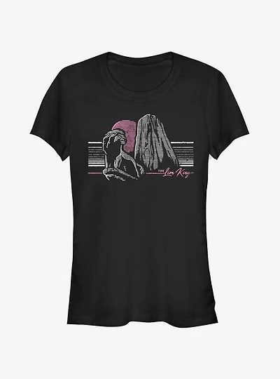
Hot Topic
Disney The Lion King Rock Lines Girls T-Shirt
Current price:
$19.92
Original price:
$24.90
From Hot Topic
Wishlist
Add To Wishlist
Quick View
Loading Inventory...
Loading Inventory...
Hot Topic
Disney The Lion King No Worry Lines T-Shirt
Current price:
$19.12
Original price:
$23.90
From Hot Topic
Wishlist
Add To Wishlist
Quick View
Loading Inventory...
Loading Inventory...
Lurking Class by Sketchy Tank
Lurking Class by Sketchy Tank Barbed Stripe Black & Grey Beanie
Current price:
$19.99
Original price:
$29.95
From Zumiez
Wishlist
Add To Wishlist
Quick View
Loading Inventory...
Loading Inventory...
Barnes & Noble
Design for Manufacturability: From 1D to 4D 90-22 nm Technology Nodes
Current price:
$109.99
From Barnes & Noble
Wishlist
Add To Wishlist
Quick View
Loading Inventory...
Loading Inventory...
Barnes & Noble
Circuit-Technology Co-Optimization of SRAM Design Advanced CMOS Nodes
Current price:
$119.99
From Barnes & Noble
Wishlist
Add To Wishlist
Quick View
Loading Inventory...
Loading Inventory...
Barnes & Noble
Beyond-CMOS Technologies for Next Generation Computer Design
Current price:
$129.99
From Barnes & Noble
Wishlist
Add To Wishlist
Quick View
Loading Inventory...
Loading Inventory...
Barnes & Noble
Prayers for your children's deliverance
Current price:
$19.99
From Barnes & Noble
Wishlist
Add To Wishlist
Quick View
Loading Inventory...
Loading Inventory...
Windsor
Katye Strapless Mermaid Satin Formal Dress
Current price:
$19.97
Original price:
$74.90
From Windsor
Wishlist
Add To Wishlist
Quick View
Loading Inventory...
Loading Inventory...
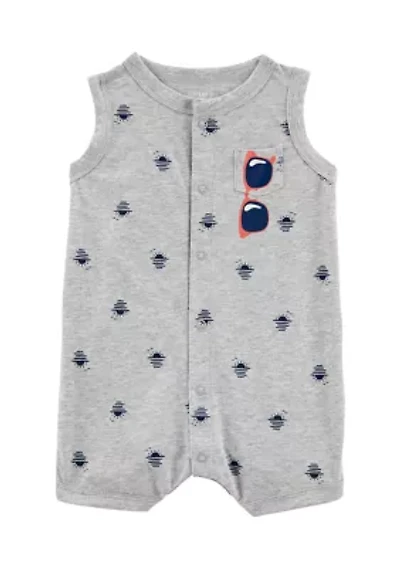
Carter's®
Baby Boys Printed Romper
Current price:
$6.40
Original price:
$16.00
From Belk
Wishlist
Add To Wishlist
Quick View
Loading Inventory...
Loading Inventory...
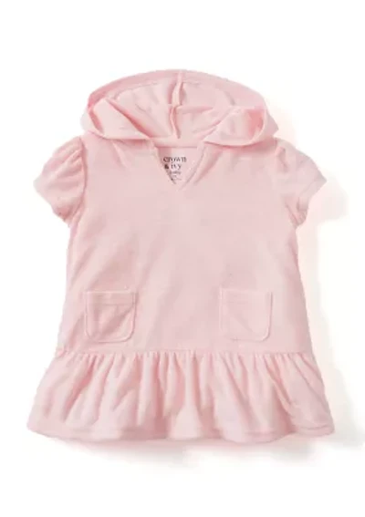
Crown & Ivy™
Baby Girls Cover Up
Current price:
$34.00
From Belk
Wishlist
Add To Wishlist
Quick View
Loading Inventory...
Loading Inventory...
Barnes & Noble
The Unlikely Spy
Current price:
$44.99
From Barnes & Noble
Wishlist
Add To Wishlist
Quick View
Loading Inventory...
Loading Inventory...
Barnes & Noble
Biomedical Quality Auditor Handbook
Current price:
$142.00
From Barnes & Noble
Wishlist
Add To Wishlist
Quick View
Loading Inventory...
Loading Inventory...
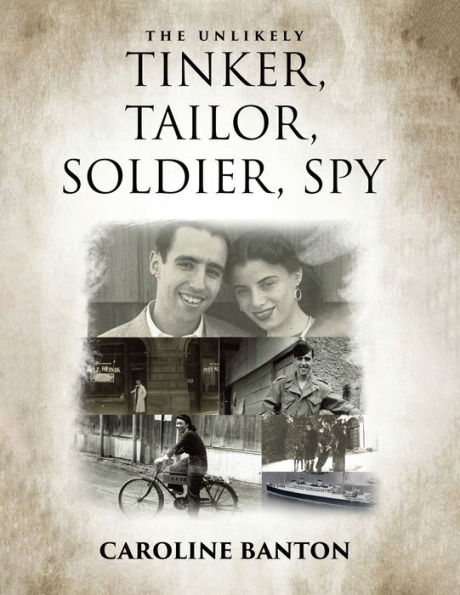
Barnes & Noble
The Unlikely Tinker, Tailor, Soldier, Spy: Soldier, Spy: Soldier, Spy
Current price:
$32.00
From Barnes & Noble
Wishlist
Add To Wishlist
Quick View
Loading Inventory...
Loading Inventory...
Barnes & Noble
Refugee Crisis in International Policy Volume II - Refugee Policies of The EU and European Countries
Current price:
$30.71
From Barnes & Noble
Wishlist
Add To Wishlist
Quick View
Loading Inventory...
Loading Inventory...
Windsor
Sleek And Stylish Moves Catsuit
Current price:
$6.97
Original price:
$39.90
From Windsor
Wishlist
Add To Wishlist
Quick View
Loading Inventory...
Loading Inventory...
Express
Double Pocket Linen-Blend Short Sleeve Shirt
Current price:
$24.97
Original price:
$68.00
From Express
Directory
Search
Scroll to Top
Close
Visit Bunny
Directory
Products
Deals
Events
About
(opens in a new tab)
(opens in a new tab)
Leasing
Close