Home
Point and Extended Defects in Semiconductors
Barnes and Noble
Loading Inventory...
Point and Extended Defects in Semiconductors in Franklin, TN
Current price: $54.99
Barnes and Noble
Point and Extended Defects in Semiconductors in Franklin, TN
Current price: $54.99
Loading Inventory...
Size: OS
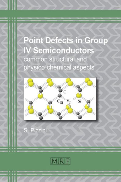
The systematic study of defects in semiconductors began in the early fifties. FrQm that time on many questions about the defect structure and properties have been an swered, but many others are still a matter of investigation and discussion. Moreover, during these years new problems arose in connection with the identification and char acterization of defects, their role in determining transport and optical properties of semiconductor materials and devices, as well as from the technology of the ever increasing scale of integration. This book presents to the reader a view into both basic concepts of defect physics and recent developments of high resolution experimental techniques. The book does not aim at an exhaustive presentation of modern defect physics; rather it gathers a number of topics which represent the present-time research in this field. The volume collects the contributions to the Advanced Research Workshop "Point, Extended and Surface Defects in Semiconductors" held at the Ettore Majo rana Centre at Erice (Italy) from 2 to 7 November 1988, in the framework of the International School of Materials Science and Technology. The workshop has brought together scientists from thirteen countries. Most participants are currently working on defect problems in either silicon submicron technology or in quantum wells and superlattices, where point defects, dislocations, interfaces and surfaces are closely packed together.
The systematic study of defects in semiconductors began in the early fifties. FrQm that time on many questions about the defect structure and properties have been an swered, but many others are still a matter of investigation and discussion. Moreover, during these years new problems arose in connection with the identification and char acterization of defects, their role in determining transport and optical properties of semiconductor materials and devices, as well as from the technology of the ever increasing scale of integration. This book presents to the reader a view into both basic concepts of defect physics and recent developments of high resolution experimental techniques. The book does not aim at an exhaustive presentation of modern defect physics; rather it gathers a number of topics which represent the present-time research in this field. The volume collects the contributions to the Advanced Research Workshop "Point, Extended and Surface Defects in Semiconductors" held at the Ettore Majo rana Centre at Erice (Italy) from 2 to 7 November 1988, in the framework of the International School of Materials Science and Technology. The workshop has brought together scientists from thirteen countries. Most participants are currently working on defect problems in either silicon submicron technology or in quantum wells and superlattices, where point defects, dislocations, interfaces and surfaces are closely packed together.